Samsung's Lee Jae-yong Visits Yokohama Advanced Package Lab
Samsung Electronics Chairman Lee Jae-yong toured the Advanced Package Lab in Yokohama to review next-generation packaging research and talk cooperation with Japanese suppliers.
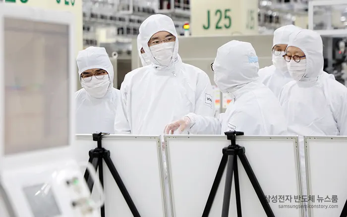
Samsung Electronics Chairman Lee Jae-yong visited the company's Advanced Package Lab (APL) in Yokohama, Japan, on November 1 to check progress on advanced chip packaging, a field that has become a key battleground in AI semiconductors. According to Samsung, it was his first on-site visit since the lab officially opened on September 8, about two months ago.
Lee reviewed the development of packaging materials and process technologies with APL researchers and discussed concrete cooperation with Japanese suppliers of materials, parts and equipment. He urged the team to secure advanced packaging technology, which he described as central to chip competitiveness in the AI era.
What the APL does
The APL develops and verifies the element technologies needed for advanced chip packages, including materials and processes. Samsung set up the lab in Yokohama in 2023 and is investing 40 billion yen (about 3.5 billion won... see note) over five years from 2024.
Its core role is to link Samsung's design and manufacturing strengths with Japan's ecosystem of suppliers. Initial priorities are wafer bonding and glass substrates, which offer better flatness and thermal stability than conventional organic substrates. Samsung also envisions expanding the lab's scope to a new packaging architecture for mass-producing low-power, high-performance AI chips.
Research areas will be divided with the packaging team under Samsung's domestic semiconductor research institute, and the two groups are meant to work closely together. Samsung plans to keep adding local researchers and build Yokohama into a global R&D base for next-generation packaging.
Why Japan, and why packaging
Japan has many world-class materials and equipment makers, a strong industry-academia-research network, and a government that treats semiconductors and AI as strategic sectors. Yokohama, next to Tokyo, offers universities, research institutes and a cluster of packaging-related suppliers, which makes hiring specialists easier.
Packaging connects chips made on a wafer to a substrate and protects them. Once seen as a back-end step, it now directly shapes bandwidth, power efficiency and heat in AI systems that combine GPUs, high-bandwidth memory and accelerators in one package. As the race for AI chips moves beyond design and fabrication into packaging, the Yokohama lab's role is expected to grow.
More from this day
See all →
Anthropic IPO filing points to a $40 trillion market: worker pay

Instinct AI agent scraps an unused motorbike in under 10 minutes

Amazon Echo Time, Dot and Studio: Alexa Plus Gets New Hardware