Neowine Patents Method to Boost HBM Yield by Discarding Bad TSVs
Korean fabless firm Neowine has patented a design that bypasses faulty through-silicon vias instead of repairing them, aiming to lift HBM yields from 30–70% to as high as 99%.
 SUMO· the number puzzle
 Dialo· learn languages by speaking
 ediviewer· read EDI files like documents
 giftdetect· the right gift in minutes
Neowine, a Korean fabless company focused on security semiconductors, says it has developed a core technology that improves yield in high-bandwidth memory (HBM) by discarding defective data paths rather than repairing them. The company has completed domestic registration of the patent, titled "High Bandwidth Memory Device" (No. 10-3036335), and has also filed in the United States.
The problem with stacked memory
HBM stacks 12 to 16 or more DRAM dies vertically and links them through thousands of through-silicon vias (TSVs). A single microscopic defect in one TSV can force the entire memory stack to be scrapped. The risk is greater once the stack has been joined to a GPU through advanced packaging such as TSMC's CoWoS, because a late-found defect means the expensive logic die is thrown away too. That is why TSV yield becomes more critical as stack heights rise.
How the patent works
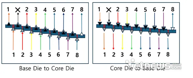
Neowine's approach provides more TSVs than needed from the start and simply routes around any that fail. The conventional fix inserts spare TSVs (RTSVs) and multiplexer switch circuits into every DRAM die. According to the company, that enlarges the die, complicates the memory-cell process and accumulates RC signal delay layer by layer, slowing operation.
Neowine instead concentrates the path-selecting switches in a single place, the bottom base (buffer) die. The DRAM dies stay unchanged, which limits die area and process burden, while signal control is handled in the base die's fine logic process. Adding more spare paths also lets the design cope with multiple faults, such as two adjacent lines shorting. The company says HBM process yields, which typically sit at 30–70%, could reach as high as the 99% range.
Timing with HBM4
Starting with sixth-generation HBM (HBM4), I/O paths double from 1,024 to 2,048, sharply raising TSV density. At the same time, memory makers are moving base dies from their own DRAM processes to foundries' leading-edge logic processes, which makes it easier to pack switch logic into the base die. CEO Lee Hyo-seung said the shift of base dies to logic foundry processes lines up well with the patent's approach.
Apps worth a look
SUMO: the number puzzleTap the right tiles, add them up, hit the target. Easy to learn, hard to master. Free, for all ages.
Dialo: learn languages by speakingTalk to an AI conversation partner; every sentence comes back corrected and explained in your language. 9 languages, A1 to C2.
ediviewer: read EDI files like documentsOpen EDIFACT and X12 messages, see every segment explained, convert to JSON/XML, export PDF and Excel. Runs locally, no upload.
giftdetect: the right gift in minutesPick who it is for, the occasion and their personality. The search engine reads product descriptions from local shops and ranks what fits. Free, no sign-up.
More from this day
See all →
Citus Demonstrates GPS-Free Firefighter Tracking, Eyes Military Use

Google Cloud expands CodeMender and AI agent security tools

Operation Ghostbusters: 830,840 Suspected Ghost Students Found