Z2RAM: Pat Gelsinger Backs Memory Meant to Break the Memory Wall
Former Intel chief Pat Gelsinger is investing in Nagare Labs and its Z2RAM, a stackable memory that promises SRAM-class bandwidth with density closer to DRAM.
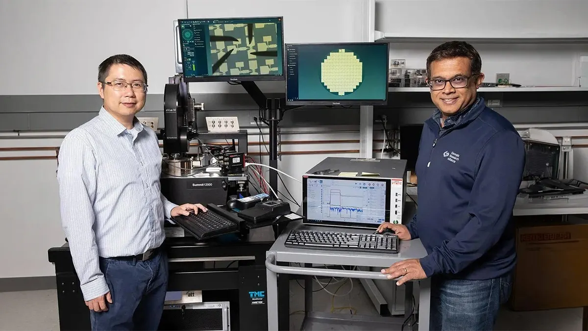
Pat Gelsinger, the former head of Intel, is putting money behind a technology that targets one of the biggest bottlenecks in modern computing: getting data to processors fast enough. The technology is Z2RAM, developed by the startup Nagare Labs. On paper it combines SRAM speed, near-DRAM density and NAND-style vertical stacking. For now, the key words are "on paper".
The memory wall
Processors and AI accelerators keep getting faster, but memory has not kept up. Over the past three decades, peak compute performance has grown by about 70% a year, while memory bandwidth has grown by roughly 20%. The result is compute units that sit idle waiting for data.
Generative AI makes this worse, because large models constantly shuffle huge volumes of parameters between memory and execution units. Each transfer costs time and energy. Nagare Labs claims that fetching a value from HBM can use around a thousand times more energy than computing on it. That figure comes from a company promoting an alternative, so it should be read as a vendor claim.
What Z2RAM promises
Nagare Labs is a Georgia Tech spin-off co-founded by professors Suman Datta and Shimeng Yu. Datta helped develop High-k/Metal Gate and Tri-Gate transistors used by Intel. Yu created NeuroSim, an open-source simulator for new memory architectures.
A classic SRAM cell needs six transistors per bit, which eats a lot of silicon. DRAM is denser but lacks SRAM's speed. Z2RAM drops the physical capacitor and uses two transistors, storing charge in the gate capacitance of the second. That makes reads non-destructive, which should reduce latency. The design is based on oxide semiconductors, with memory layers stacked directly above the accelerator and no interposer. Vertical connections would span the whole surface, so data travels micrometers rather than millimeters. The company targets transfer energy well below one picojoule per bit.
The first generation aims for five times SRAM density using six layers, with a roadmap reaching beyond 100 layers. In the space of a 64 MB SRAM tile, Z2RAM would fit about 320 MB at comparable bandwidth, according to the company. The approach resembles AMD's 3D V-Cache in spirit, though Nagare Labs is aiming considerably higher.
All of these figures are goals and claims, not specifications of a shipping product. Whether Z2RAM can reach production at a competitive cost is still unproven.
More from this day
See all →
Philip, the invented ghost that 1970s Toronto researchers made talk

Web tool calculates your age on every Solar System planet

Apple Watch Audio Intelligence may violate US wiretap laws

NASA Keeps Mars Odyssey and MRO Running 25 Years On
More in: Hardware
See all →
Sam Altman Calls Home PC RAM for Local AI 'Pretty Terrible'
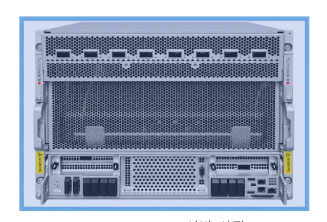
DS&G Backs Korea University's InThon Hackathon With Nvidia B300 Servers

GEX Pure Pet Fur Sweeper Collects Cat Hair Around the Clock