Frostbite: an AI-designed CPU claims 4.59x better performance per watt
Architect Labs says an AI designed Frostbite, a CPU architecture with no legacy baggage, and that it beat an unnamed conventional core by 4.59x per watt in simulation.
 SUMO· the number puzzle
 Dialo· learn languages by speaking
 ediviewer· read EDI files like documents
 giftdetect· the right gift in minutes
Frostbite is a general-purpose CPU architecture that, according to its makers, was designed from scratch by artificial intelligence. The US startup Architect Labs says it beat a conventional processor core by an average of 4.59 times in performance per watt. The rival core is not named, which the company reportedly puts down to legal reasons.
The pitch is simple. Today's desktop and laptop chips carry decades of compatibility baggage: old instruction sets and design decisions that cannot be thrown out without breaking software. That costs performance and power. A clean-sheet design skips all of it.
How does the Frostbite CPU work?
Frostbite is built on interaction nets, a model of computation proposed back in 1990. A program becomes a graph of connected nodes, and every value has one owner and is used exactly once. Because the links between operations are spelled out, independent tasks can run in parallel without out-of-order execution, the trick normal CPUs use to juggle instruction dependencies.
The chip is made of compute tiles that pass work to each other over an on-chip network. An idle tile can grab work from a neighbour, or go to sleep to save power. Programs are written in a Rust-like language called Vine, which a compiler turns into an intermediate form called Ivy.
What did the AI actually do, and how fast is it?
The design ran through the company's own formal specification system, ASL, plus a model called Arcmodel. The description of 31 hardware blocks became more than 800,000 lines of formal specs. Arcmodel simulated power and speed about 660 times faster than RTL simulation. The AI considered 58 architectural changes and 37 were accepted. Some of its solutions surprised the human engineers, the company says.
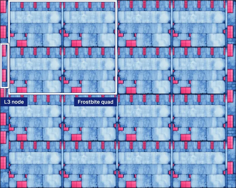
The numbers come from a 7 nm software synthesis, so there is no physical chip yet. Timing reached 800 MHz at synthesis and 500 MHz in the final layout. One Frostbite Quad cluster covers 0.792 mm², against 0.895 mm² for the comparison core.
Across 25 tests, Frostbite averaged 4.59x the performance per watt and 8.77x per unit of area. On 15 tests not used during optimisation, the energy-efficiency gain was 3.83x. Architect Labs promises wider benchmark testing later. In August it said an AI had designed its Redwood AI accelerator in two weeks, but it has not said how long Frostbite took.
Apps worth a look
SUMO: the number puzzleTap the right tiles, add them up, hit the target. Easy to learn, hard to master. Free, for all ages.
Dialo: learn languages by speakingTalk to an AI conversation partner; every sentence comes back corrected and explained in your language. 9 languages, A1 to C2.
ediviewer: read EDI files like documentsOpen EDIFACT and X12 messages, see every segment explained, convert to JSON/XML, export PDF and Excel. Runs locally, no upload.
giftdetect: the right gift in minutesPick who it is for, the occasion and their personality. The search engine reads product descriptions from local shops and ranks what fits. Free, no sign-up.
More from this day
See all →
INFOBAR ZERO: KDDI's Phone With No Internet, and Why It Made It
SBC Medical Group breach: 1.62 million records, plain-text passwords
Supermicro lawsuit: ex-exec's husband was a top Nvidia VP