Airmembrane Raises About ¥850M for Graphene EUV Pellicles
Japanese startup Airmembrane has secured about ¥850 million in equity, bank debt and a NEDO grant to mass-produce graphene pellicles for next-generation EUV lithography.
Airmembrane, a Japanese startup developing graphene pellicles for EUV (extreme ultraviolet) lithography, announced on October 30 that it has raised roughly ¥850 million in total. The round combines a third-party share allotment, a loan from Sumitomo Mitsui Banking Corporation and a grant from NEDO, Japan's public research agency. The company did not disclose the individual amounts. Cumulative funding, including equity, debt and grants, now stands at about ¥10 billion...
Who is backing the company
Global Brain led the equity portion through its Fund No. 9, the Takanawa Chikyueki fund and the Shinhan-GB Future Flow fund. A-Start, KSP (through the NextG fund) and Mitsubishi UFJ Capital also took part, the latter as a follow-on investor. The NEDO grant comes from its program supporting practical R&D and mass-production demonstrations for deep-tech startups in the GX field.
Why the pellicle matters
A pellicle is a protective component for the photomask, the master pattern used in EUV chip production. Even tiny particles landing on a mask can cut manufacturing yield sharply. An EUV pellicle must be extremely transparent to light, dissipate heat at very high temperatures, stay chemically stable in plasma and remain mechanically strong. These requirements trade off against one another, and the company says few products worldwide meet all of them at a cost suited to volume production.
The main hurdle is producing graphene, a film one carbon atom thick and hard to handle, at high quality and in volume. Airmembrane says its continuous synthesis and automated transfer technology, developed from work at Japan's National Institute of Advanced Industrial Science and Technology, addresses this. It claims synthesis speeds more than 100 times faster than conventional methods, with automated transfer removing fine defects and contamination.
Roadmap
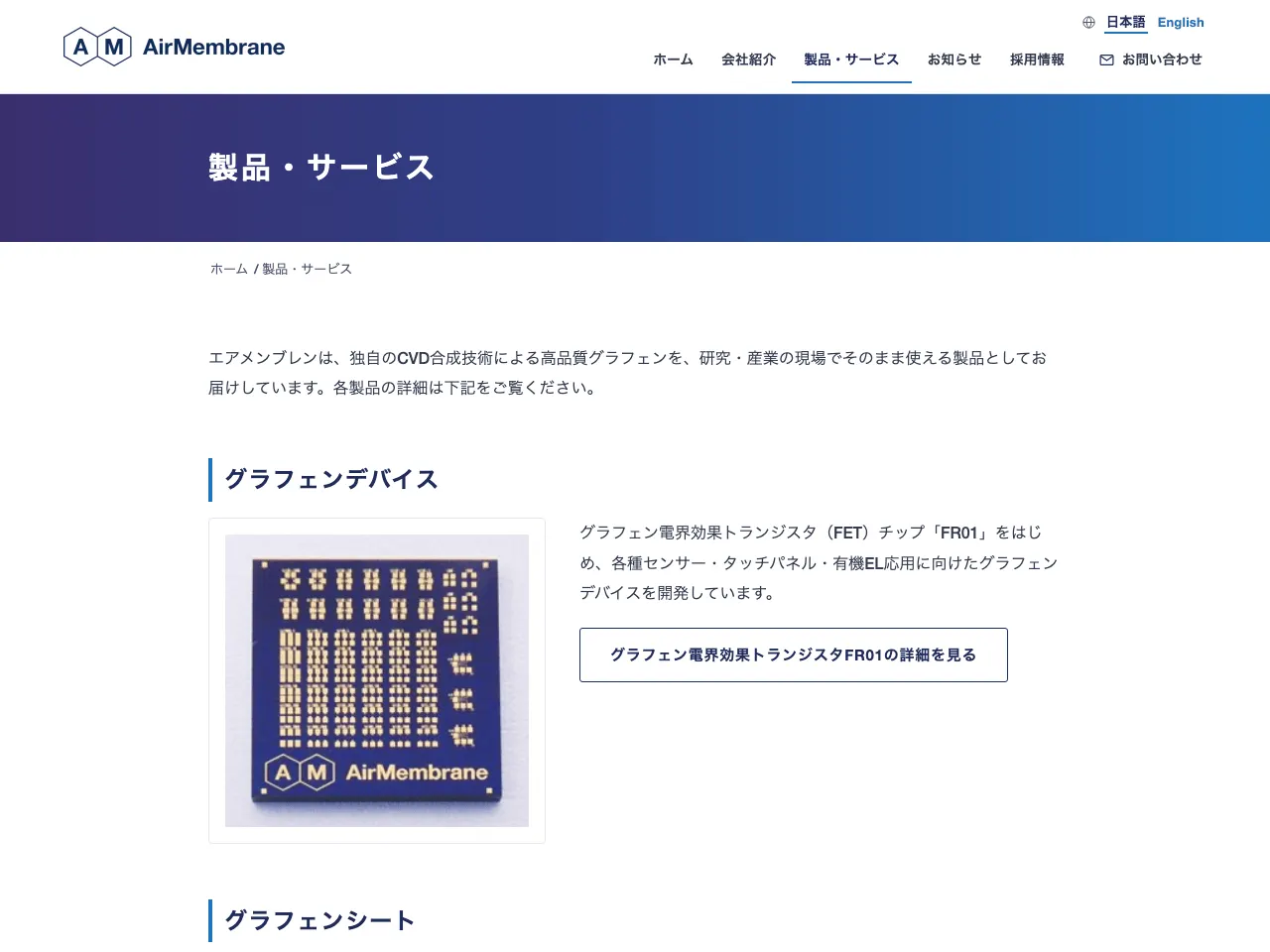
In September, director and CBO Ryo Shinomoto presented the synthesis and transfer technology and the commercialization roadmap at SPIE Photomask Technology + EUV Lithography 2026 in Monterey, California. The new funds will go toward building mass-production capacity: a measurement system to control defects, uniformity and lifetime, with pilot production in 2027, and a volume production line for next-generation EUV scanners in 2028. Airmembrane already sells CVD graphene products, including the FR01 graphene FET chip, graphene sheets, TEM grids and a UV irradiation unit.
Apps worth a look
 SUMO: the number puzzle
Tap the right tiles, add them up, hit the target. Easy to learn, hard to master. Free, for all ages.
 Dialo: learn languages by speaking
Talk to an AI conversation partner; every sentence comes back corrected and explained in your language. 9 languages, A1 to C2.
 ediviewer: read EDI files like documents
Open EDIFACT and X12 messages, see every segment explained, convert to JSON/XML, export PDF and Excel. Runs locally, no upload.
More from this day
See all →
Apple Maps Blurs Satellite Images of NASA and Air Force Sites

Instagram Tests 90-Minute Videos to Compete for Podcasts

WhatsApp Lets You Call People Who Don't Have an Account

Reddit Plans Mandatory Login to Curb AI Scraping and Boost Users
More in: Startups
See all →
Albatrus Builds Apollo AI, a Core System for Japanese Hospitals

India's Deeptech Funding Gap: Skyroot Built Rockets, VCs Hesitate

Prosus Wins India's CCI Approval for $100M Investment in Navi